In my previous post I showed you my wireless temperature and humidity sensor project which didn’t have a nice home yet. So today, I’m going to show you how I developed my own PCB to build a more useful and permanent version of my sensor, which I’ll place around my house to monitor the climate inside and outside.
There are many different ways to fabricate you own PCB’s at home, the method I choose was to use photo-resist laminate since that way I could use my inkjet printer and didn’t have to buy a laser printer (for the toner-transfer method). The basic idea is that the board is covered with a thin film of a photosensitive layer, which prevents the etching solution to reach the copper. By exposing this thin film of photosensitive layer with UV light and developing it afterwards, the photoresist layer is removed everywhere where the copper is not supposed to be. I’ll show you how it’s done in more detail now.
Building a UV Lamp
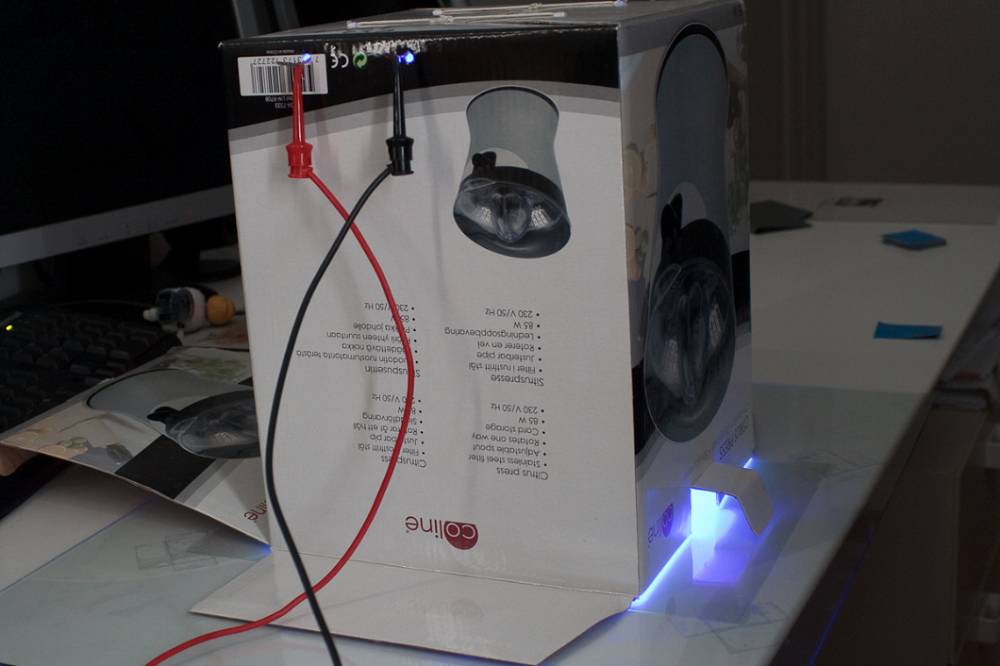
First a UV lamp is needed. Instead of buying a rather expensive professional UV exposure box, I built my own using UV LEDs. I ordered some cheap LEDs from ebay which have a wavelength of about 400nm, a strength of 7000mcd, voltage drop of 3.4V and which require a current of 20mA. I arranged the LEDs is rows of 3 with a 100Ohm resistor such that I can use a 12V DC power supply. After soldering the LEDs in a 3 x 9 x 2 formation onto a prototype board, I mounted the lamp in a box as shown on the following pictures:


Result: a fully functional UV exposure box, which consumes about 0.39A @ 12V.
Printing the art work
Next step is to design and print the PCB layout. I used the wonderful program Eagle to do this. You can download my eagle project files (including all self created library files) at the button of this page. I sized the board in such a manner that it will fit into a plastic case which I have (see below). The final result is:
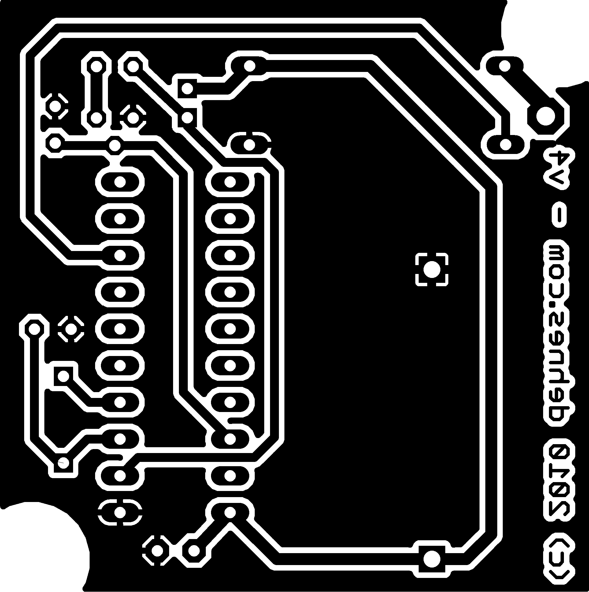
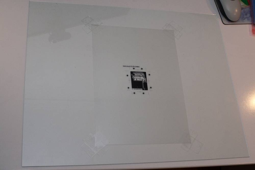
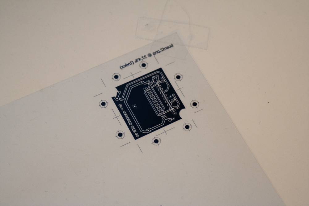
For the PCB to be a good as possible, it is crucial that your print is of good quality and has nice smooth lines. To achieve this, I exported the board layout from eagle using 1200 DPI and set the print quality to best. Then I used photoshop to actually print the file onto the transparent film (I used Transparency Film from Pelikan for my standard HP inkjet printer) because it provides the possibility to print additional orientation marks. I used those orientation marks to align two prints on top of each other, to create an even thinker layer of black, which is supposed to stop the UV light from getting to the board.
Preparing the laminate
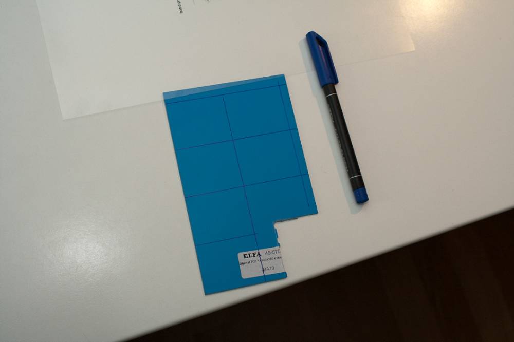
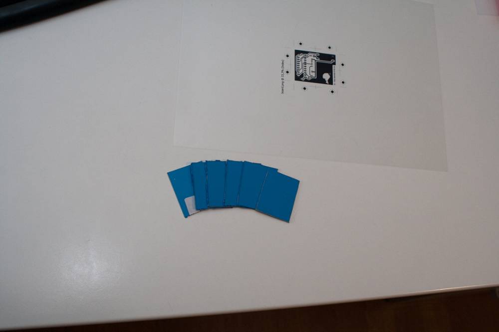
Once the artwork is prepared and taped down onto a glass plate, I prepared the laminate; the actual boards. I measured the pieces and cut them out using my Dremel.
UV exposure
Now the development can begin. To bring the layout onto the laminate, the blue protection foil is removed from the laminate and the piece is placed under the glass plate with the art worked taped onto. The UV exposure box goes on top such that the UV light hits the art work first and then the photoresist layer on the laminate. Exposure time is about six minutes.
Once done, the exposed board is placed in a chemical solution (a photo resist developer) to remove the photoresist layer at those places where we don’t want any copper to be. The result looks like this.
The darker layer on top of the copper is the photoresist layer which will prevent the etching solution to reach the copper (and thus doesn’t get etched away).
Etching the board
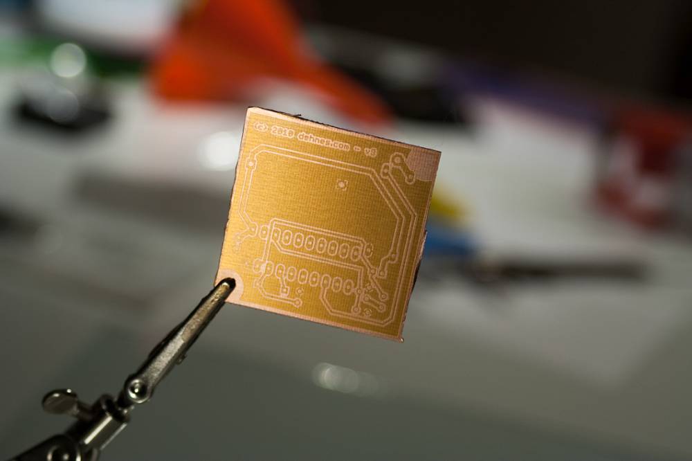
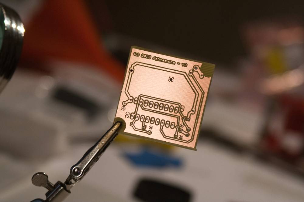
The final step of making our PCB is to etch the copper which we don’t want away. The board is placed in a etching solution (natrium persulfate) at about 40 degrees for about 20 minutes or so. Once done, I drilled the holes using my Dremel and removed the remaining photoresist layer with nail polish remover. The finished PCB result looks like this:
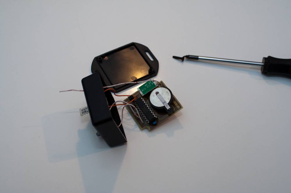
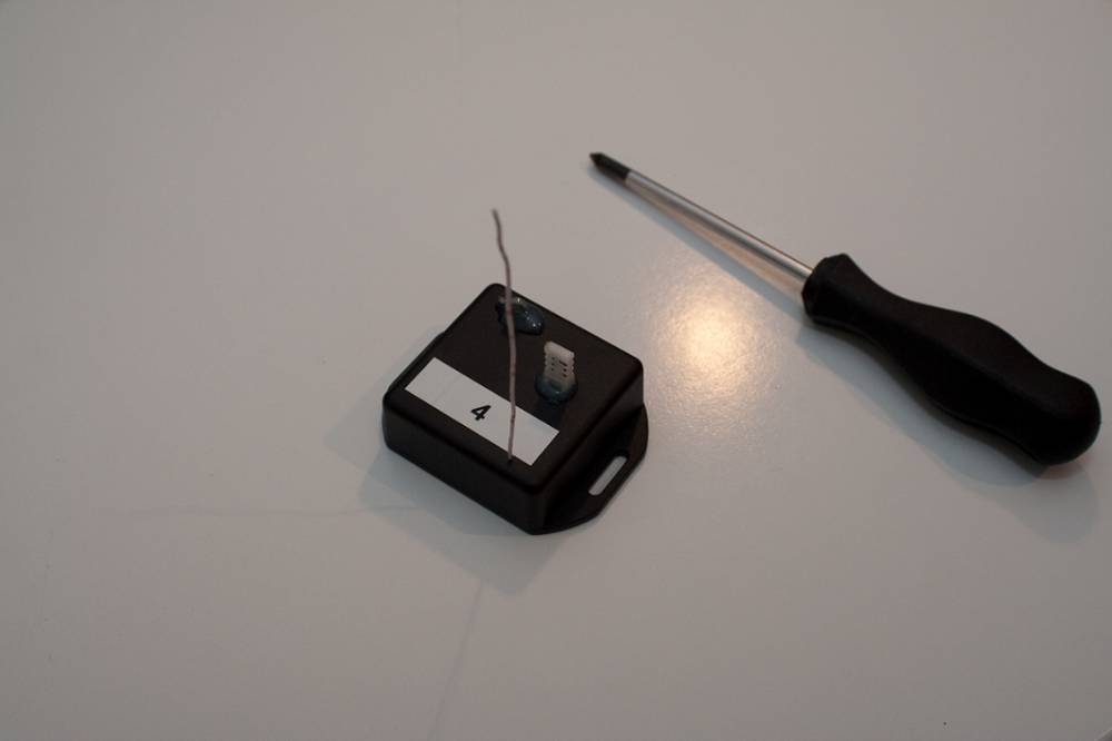
At last, I soldered all components onto the board and fitted the board into a small plastic housing, which it will live in. The temperature and humidity sensor are clued on the outside of the case, such that they are in contact with the air outside. The finished sensor looks like this:
Result
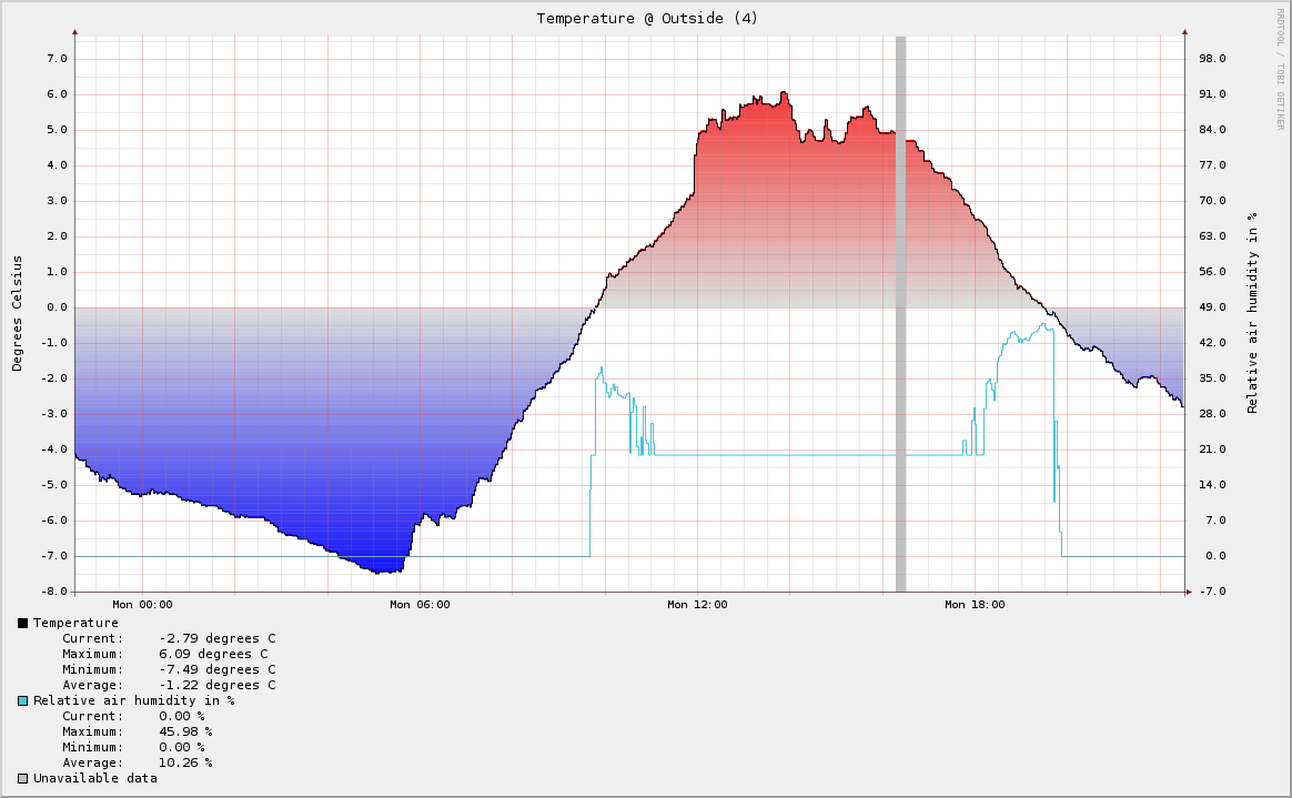
I installed two sensors outside at places where the sun doesn’t reach them both at the same time. Using rrdtool, the following graph was generated by combining the data from the two sensors (assuming the coldest temperature reading is the correct one):