In this blog post, I wrote about my sensor project which transmits it’s measurements via a 433Mhz wireless communication link. On this page I will describe the details of my self built receiver which receives data from this sensor.
Goal
To build a general purpose RF receiver module which receives messages from a 433 Mhz wireless link (for example from my self built RF sensor) and forward the received and decoded message to my Linux server via USB, where they are further processed.
Scope
- A AM-RRQ3-433 from RF-solutions is used to receive raw signals from the 433Mhz RF channel
- For the USB interface, I'll be FTDI's TTL-to-USB cable, which is a ready-to-use solution for briding 5V TTL signals to RS232 emulation over USB. This enables the microcontroller talk directly to the linux box without any additional components. The linux kernel supports the FTDI chip, so it works out of the box. When this cable is plugged in, the RS232 port is reachable via /dev/ttyUSB0.
- This cable also provides also a 5 Volt power source which will be used to power the entire receiver module.
- For debugging purposes and possible other future features, the receiver module will be able to write to a HD44780 compatible display (I’ll be using the EAW162B-N3LW) which is attached using a 14 channel flat cable
- A potentiometer is used to provide a configurable reference voltage for the purpose of noice filtering.
- For the main processor, a PIC16F690 microcontroller will be used, which has a built-in crystal/clock and enough pins to support all interfaces described above.
- For re-programming the firmware of the microcontroller without needing to remove the chip from the board, I’ll be using ICSP (In-Circuit Serial Programming)
Protocol
All messages which this receiver module should be able to receive are encoded in my own RF protocol. This protocol is a kind of Ethernet protocol, it contains a destination address field, a source address field a message length and a checksum field. This protocol does not say anything about the kind of content which it carries. The syntax looks as follows:
| Position | Contains | Length in number of bits |
|---|---|---|
| 1 | destination (e.g. receiver’s address) | 8 |
| 2 | source (e.g. sender’s address) | 8 |
| 3 | Message's length | 8 |
| 4...N | message’s body | (N-3) * 8 |
| N+1 | CRC16 value | 16 |
When transmitted over RF; the message is encoded using Manchester encoding which is a self-clocking signal where each bit is actually sent using two bits. The length of a low-level bit is 0.5 ms which means that each logical bit takes 1 ms to transmit. At the beginning of each message, there is a start bit sent with the value of HIGH for 0.5ms.
Understanding the raw RF signal
The hardest part of this project was to translate the raw signal, which the AM-RRQ3-433 provides, to a usable message and disregard any noice and foreign signals.
The main idea here is that the RSSI port of the AM-RRQ3-433 module is used directly as a signal source (instead of the DATA-OUT port). The RSSI port is an analog port which provides both signal strength information and the information in the signal itself, whereas the DATA-OUT port is a digital port and only provides the digital signal received via RF. The DATA-OUT port will raise to HIGH (=5V) on the slightest noice on the RF channel, while the RSSI port will output a voltage which tells us about how strong the receive signal actually is. So by measuring the output voltage of the RSSI port using AD (analog-digital conversion), it is possible to both receive the signal itself and also the strength of this signal.
So when the microcontroller is receiving a signal from the RF module, a configurable reference voltage provides the minimum required voltage (signal strength) which the RSSI port has to output in order for the microcontroller to recognize this as a HIGH (1). Any voltages which the RSSI port outputs which are below this configurable reference voltage are seen as a LOW (0) by the microcontroller.
The next step after this noice filtering is to translate the received HIGH’s and LOW’s into a understandable message. In the attached source code, I’ve implemented a decoder for manchester encoding which is based on the finite-state-machine concept. A state machine is ideal to keep track of the current received bit and to determine which is the next expected next bit. As soon as a mismatch is found, a bit lasts too long (timeout case) or the max message length is exceeded, the state machine goes into error state and further reading is given up.
When the state-machine was able to decode an entire message, the next step is to calculate a CRC16 checksum over the entire message (all fields, except the CRC16 fields) and compare this value to the CRC16 fields in the message. If the CRC16 values are the same, the next step is to determine whether this messages was intended for this receiver at all. This is done by comparing the destination address in the message against a locally hardcoded address.
In case the destination address matches, the message is then forwarded over the RS232 interface to the linux box. This is done by simply sending the message over a digital output port (port RB5, see below) of the microcontroller which is connected to the TTL-to-USB cable.
The hardware
All components will be placed on a PCB board which is placed in a plastic container with an antenna on top. Here is the schematic of the board:
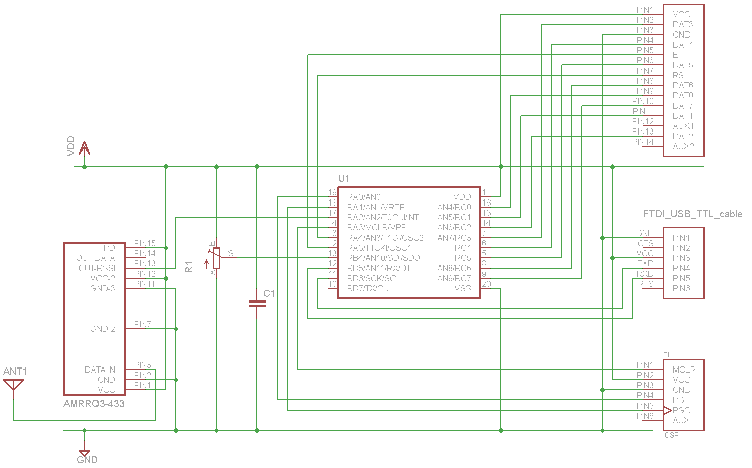
On the left side is the RF module (AM-RRQ3-433). The R1 is a 10KOhm potentiometer for configuring the RSSI reference voltage. U1 is the PIC16F690 microcontroller. In the right upper corner you find a 7×2 flat cable connector which is the connection to the display. Below is the TTL-to-USB cable connector and in the right bottom corner is the ICSP connector.
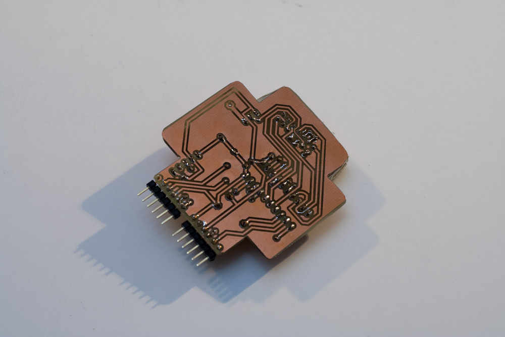
Since I wanted to fit the board into a 59mm x 59mm box, I was forced to use a double layered PCB board. The bottom layer looks as follows:
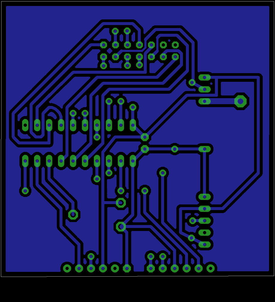
And the upper layer:
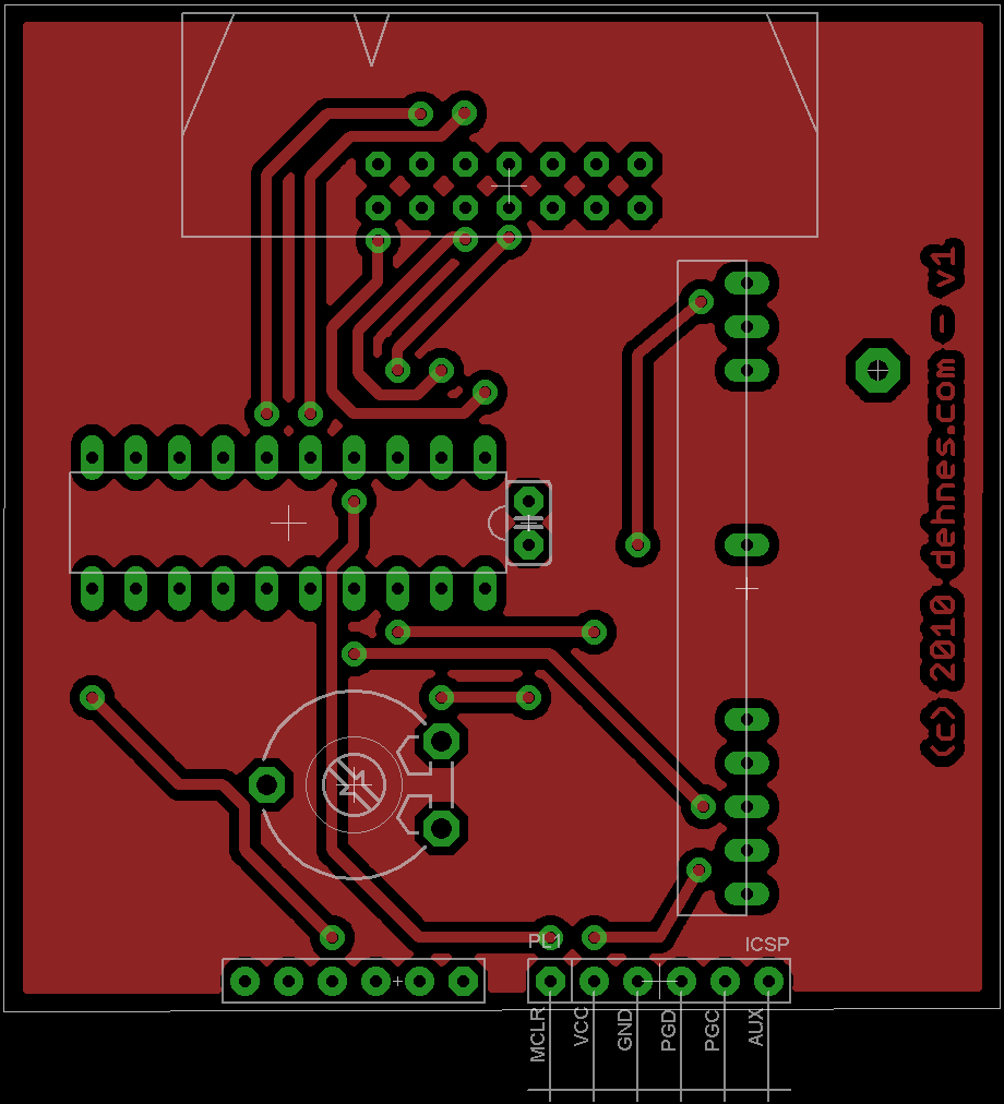
The component at the top is the 2×7 flat cable connector. The long vertical component to the right is the RF module (AM-RRQ3-433). The the PIC is in the middle and below it is the potentiometer. The 6 pin connector in the left bottom corner is the TTL-to-USB cable connector and the 6 pin connector in the right bottom corner is the ICSP connector. All other holes are vias which connect the bottom layer to the upper layer.
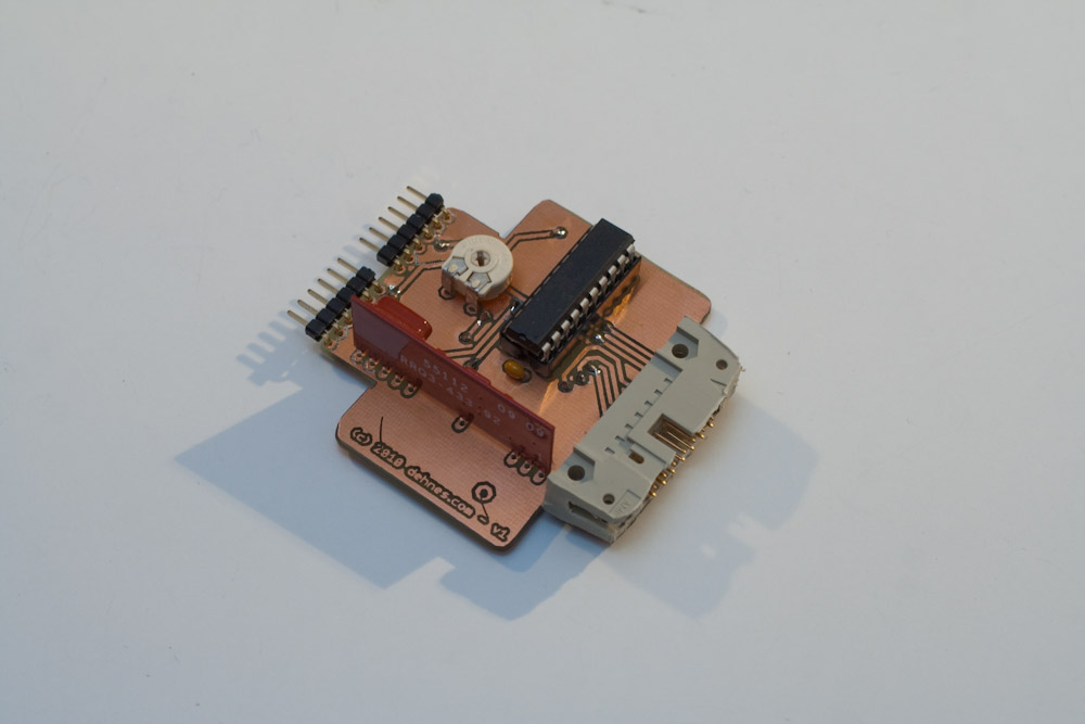
I developed the PCB using the same method as explained on my previous post with the additional feature of adding an aligned upper layer. After four attempts, I finally managed to developed a double sided board which works:
More pictures
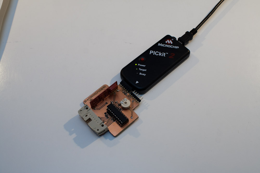
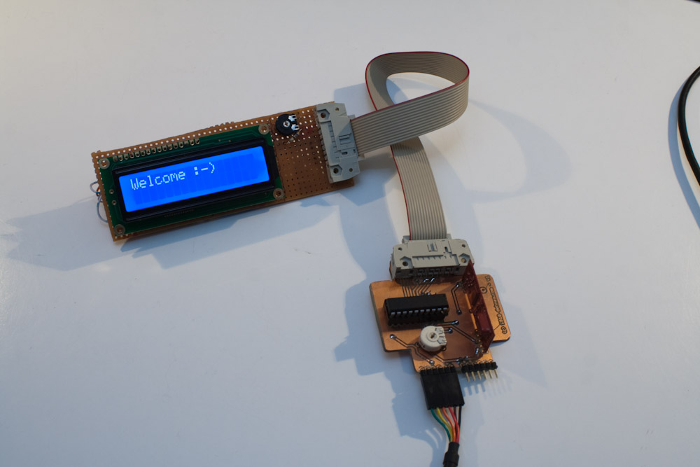
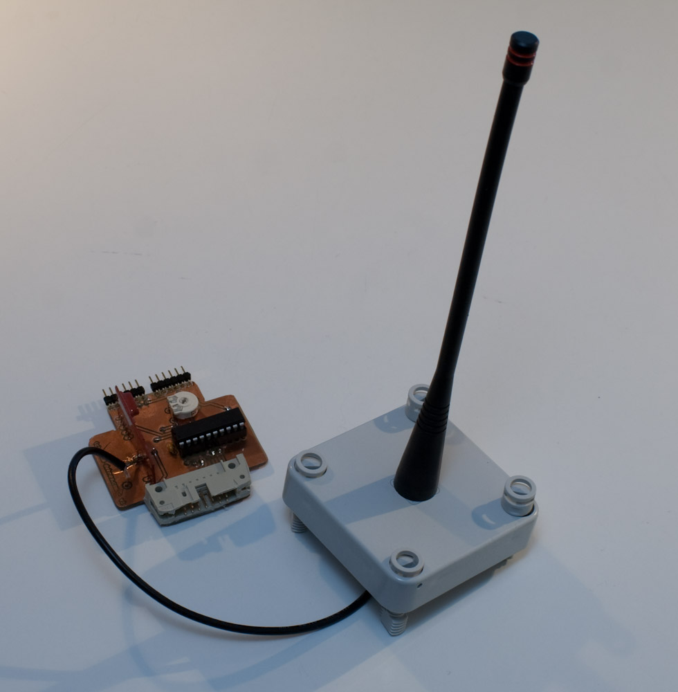
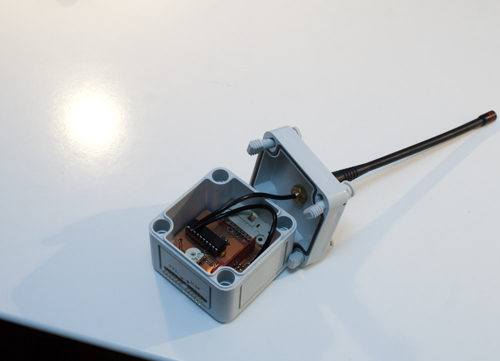
The antenna which I use is: ANT-433-PW-QW-ND.
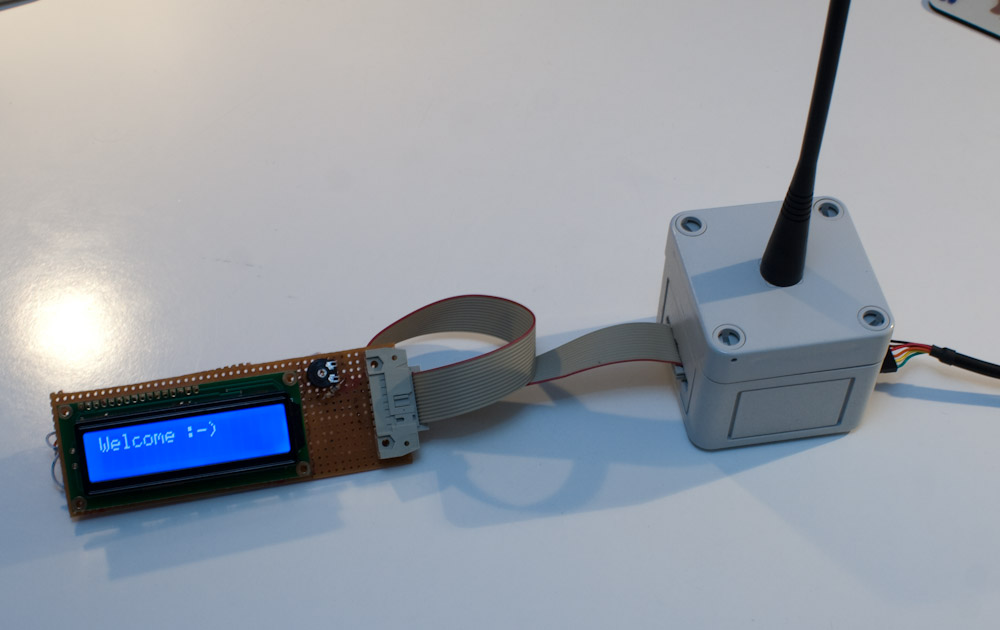
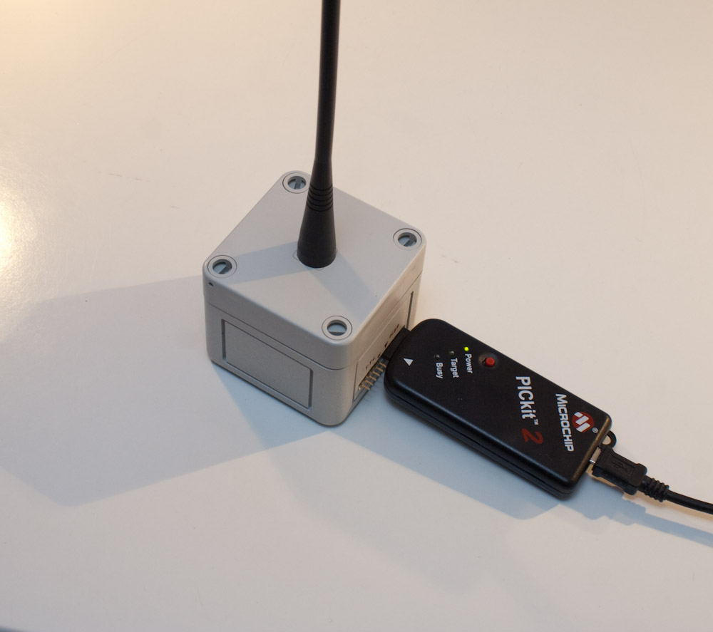
Downloads
In case you want to build something like this yourself, here are all my project files, including the source for the program on the microcontroller. I developed this using the Microchip MPLAB IDE.
- The binary executable for the PIC16F690 microcontroller: rf_receiver-v1.hex
- The assembly source code: rf_receiver_source-v1.rar
- The eagle project files: RF_receiver_eagle_files-v1.rar